3D Manufacturing of Inorganic Materials and Devices
LP3 focuses on inorganic inks for devices manufactured by laser printing of metals, semiconductors and isolators.
Click on the images to enlarge them and view the source.
Our Goal
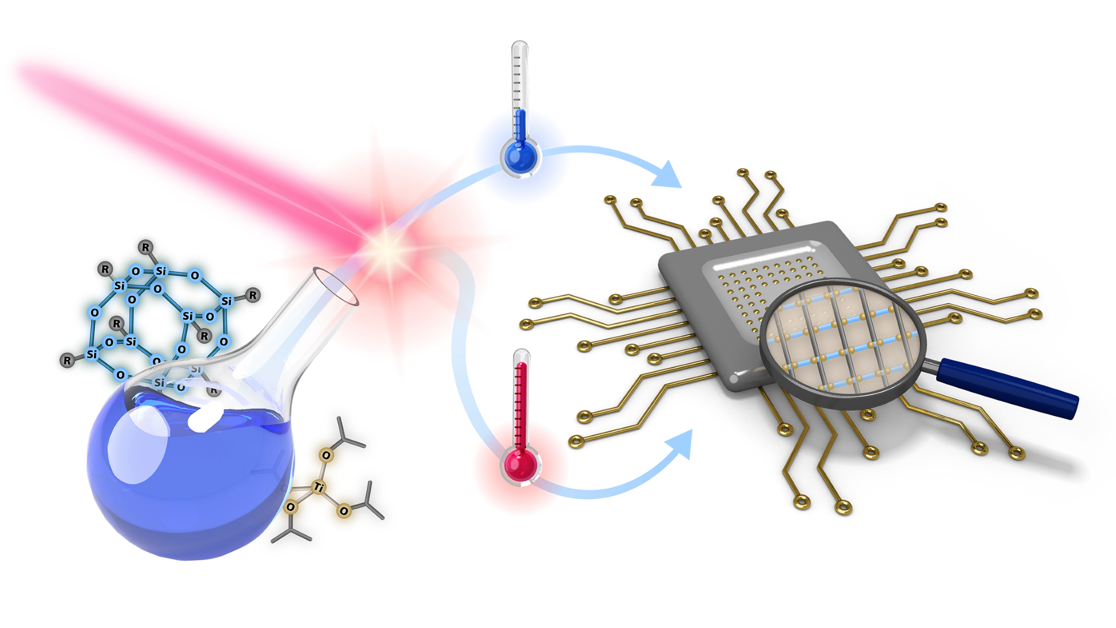
In LP3, we seek to expand the bandwidth of the most technologically important materials accessible via 3D laser nano-printing, semiconductors, metals, isolators and functional glasses. In this, we engineer novel printable feedstock materials and precursor inks, which incorporate molecular clusters of the targeted inorganics. We further develop laser printing technology to facilitate the fabrication of micro- and nanoscale three-dimensional designs for next generation device concepts. Specifically, we pursue two fundamental mechanisms; (1) the direct photo-thermal formation during 3D laser nanoprinting; and (2) the thermal conversion in a separate post-print treatment.
We will develop materials with properties including metallic, semiconducting and insulating properties, as well as ion-conducting materials. The inks for 3D laser printing should be orthogonally print compatible, enabling unrestricted design and the realization of multi-material electronic devices.
We target microscale 3D free form architectures for microoptics and electronic devices, in particular, aiming to realize field effect transistors, memristors and capacitors as well as microlenses.
We aim to explore laser-printed memristors and transistors for crossbar circuit architectures in artificial neural networks.
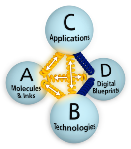
We will employ a twofold strategy. First, we will apply high-level synthetic chemistry to adopt potential precursors in terms of the desired elemental composition to the needs of the printing process. Second, to identify suitable ink designs and process parameters from the virtually infinite space of possibilities, we leverage AI-based models in combination with time- and spatially-resolved cross-scale material analyses techniques combining the strengths of all four Research Areas A, B, C, and D.
With LP3, we expect to lay the groundwork for complex multi-material stacks and functional electronic and optical devices that can lead to fully integrated photonic chips for sensing and information in the future.
Principal Investigators Involved
Jasmin Aghassi-Hagmann Karlsruhe Institute of Technology (KIT)